
I started the hardware design of the Ruby816 board based on the Ruby6502 board. It wasn’t hard to make the necessary changes and adapt the PCB layout, but at the same time, this was in-mind:
Documentation (sometimes incorrect or lacking), experiences, stories, and existing designs using the ‘816 are abundant but with that also comes conflicting tales, and at times seemingly scarily and daunting articles punctuated with stories of bus and timing conflicts, the criticality of using a transparent latch, bi-directional buffers, TTL types to avoid and ones you must use, PCB layout considerations and so on. I took the suck it and see approach and my board worked more or less first time, and like my Ruby 6502 board the 816 works at 16Mhz. It is a simple board with 512KB of RAM and a 65C22 VIA and 2 GALs in addition to the ATmega “host” processor. If you’re familiar with the BBC Micro, then one way to look at it is that the ATmega is the BBC Micro handling screen, keyboard, filing system, etc. and the ‘816 side is a Tube processor system.
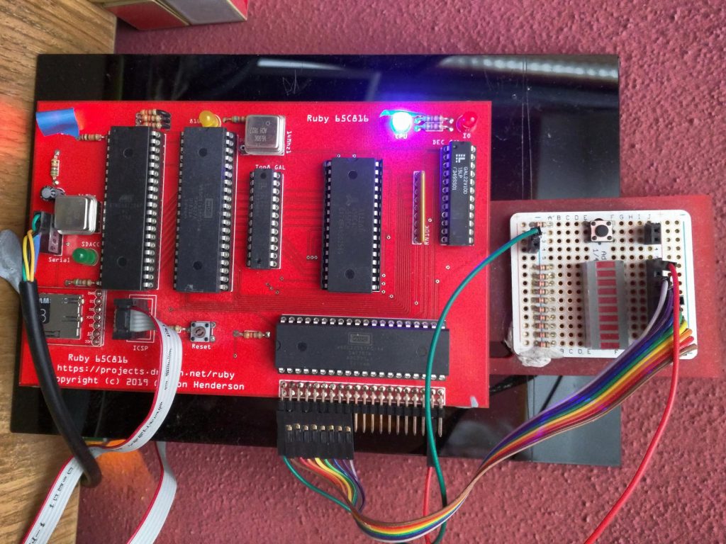
Ruby 816 board with the LED board
This is the Rev 1 Ruby816 board. From left to right: The ATmega 1284p host processor. This is clocked from a 16Mhz can oscillator (to it’s left), has a serial port and a micro SD card (which is in a carrier board which also does the voltage level shifting from Ruby’s 5v to the SD cards 3.3v) Under the ATmega is the usual ICSP programming header (There is no bootloader, I program it directly via a USB programmer)
Next is the WDC 65C816 CPU and to the right of that is the “Φ2” 16Mhz can oscillator and the “Top-8” GAL. This GAL latches the top 8 bits of the address bus at the correct time in the cycle. It also acts as an IRQ combiner as the WDC 65C22 no-longer works in pull-down/wire-or mode.
The 512KB RAM chip is next then the address decoder GAL. This provides the 256 byte IO window at $FE00 in bank 0 (it has an input from the Top-8 GAL to let it know when it’s in Bank 0 or not)
At the bottom is the WDC 65C22 VIA chip. This is used to generate a 1000Hz timer tick and for the GPIO pins – here just driving some LEDs, but I have plans for a peripheral type bus in the future.
The resistor network pulls A[8:15] high and this is needed to allow the ATmega to share the top 256 bytes of RAM in bank 0. This is where the hardware vectors are and there the ATmega pokes the bootloader. This is the same as the way the Ruby6502 boots – ATmega disables the 65816, connects to RAM, loads small bootloader, lets the 65816 run then communicates via the shared ram window.
There is really not much more to the hardware than that. I deliberately kept it as simple as I could and reduced chip count with the GALs. The PCB is double sided and all the decoupling capacitors are inside the chip sockets.