I recently thought it might be a good idea to make up a PCB of one of my Pi projects – the ladder game.
So famous last words: How hard can it be?
Fortunately, it’s not that hard now, and there is a plethora of software available to help you do the design and layout – I’d already started with the Fritzing package to produce the breadboard layouts, so I decided to stick with that. Fritzing also offer a PCB prototyping service too, which is on the expensive side, but they all are when you’re just wanting a small number of PCBs (want 1000? Sure, then the price can drop to under £2, but want one or 2 then expect to pay well over £50 for them!)
However, while using the Fritzing software (under Linux of-course), I decided to not use Fritzing for the PCB manufacture in the end – a few issues, one as that I won’t use PayPal, another was that my bank (NatWest) were just being obtuse and seemingly doing everything they could to block a money transfer to Germany (as well as charging me a stupid amount of money to do the actual transfer!) So in the end, wanting to do this quickly before I went on holiday, after a very quick search, I found PCB Panel who are based in Dorset – not the cheapest, but they base their manufacturing on making an entire panel of the same design – so I ended up with 3 PCBs from their smallest panel.
Fortunately there is a standard for conveying PCB layout data called Gerber Format and the Fritzing software can create a “Gerber” which is really a collection of various files which I could ZIP up and sent to PCB Panel for manufacture.
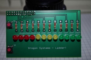
So cost aside, lets quietly ignore that for now… Turning a breadboard layout into a PCB design was rather interesting. For one, I found the routing of the wires to be somewhat challenging – until I remembered that I was making a double sided board and that it didn’t really matter which GPIO pins I actually used to drive the LEDs – I can fix that up in software later! So the final board has the 12 LEDs wired up in what may initially appear to be a random pattern, but in practice it works well.
And here it is:
You may notice a 2nd button on the board compared to the original on a breadboard – no real reason there other than “because I can”.
So what went wrong… You can probably tell from the photo that the silk-screen is somewhat incorrect. I actually did correct it, but in my rush to get things going before I went on a holiday, I emailed the wrong version to the PCB company.
The other thing is the holes for the edge connector – they’re too small. My fault for not checking the Raspberry Pi template I was using, however I’ve reported this back to the person and it turns out he had the same issues too, but it’s now been corrected.
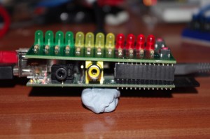
The other issue that’s not apparent is that you need an extra-long 2×13 way edge connector to make it mate with a Raspberry Pi! Standard ones are too short – which is why the PiFace is the shape it is, as it sits underneath the Pi’s Ethernet, USB and composite video connectors.
See the image above for details of the connector – and note the need for an extra long one! (If anyone knows of a UK source, please let me know!)
So there you have it. Designed and had a PCB manufactured and it’s the first time in over 25 years I’ve done that and although there are lessons to be learned, I’m actually very happy with the results.
And so tomorrow I’ll design a PCB for the next Raspberry Pi 😉


